At the end of November last year we wrote about a 10 W PA design using the AFM907N transistor. The parts arrived just before Christmas, and now that we have finally shaken off the post-holiday inertia, we are ready to bring up the board.
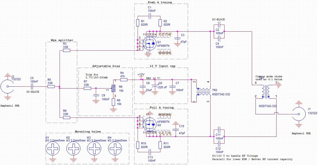
Our goal with this prototype was to see how the transistor would perform, and to see if the common mode choke amplifier topology would be viable. After testing the device, we figure that this transistor would be most suitable as a final or intermediate stage in a more integrated transceiver design. We won’t provide the blueprints for this board, since we discovered that it has some issues. Instead, we will focus on some measurements and talking points that could be of interest when using this device.
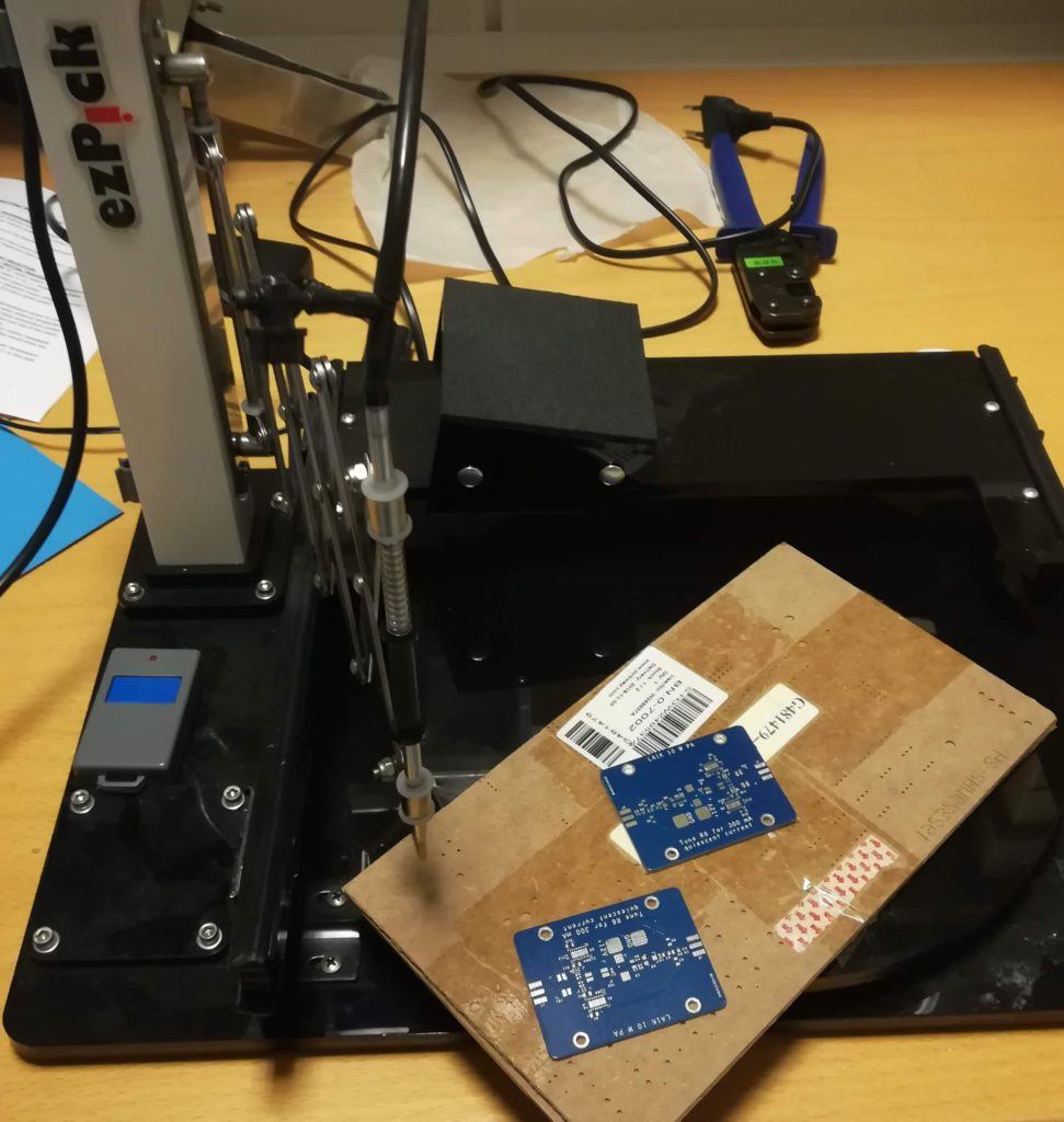
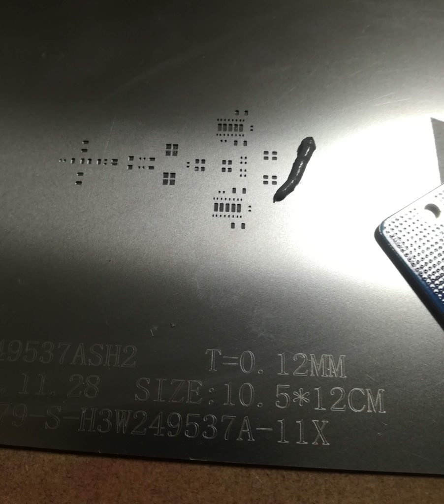
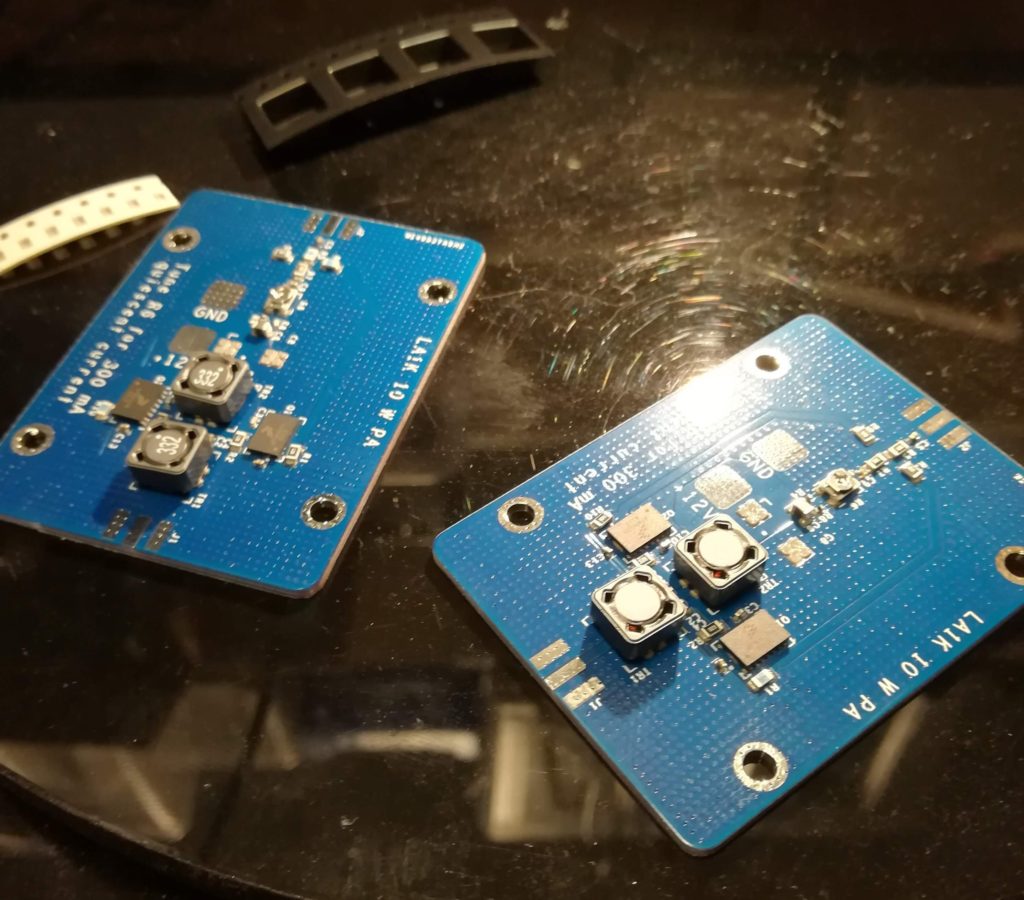
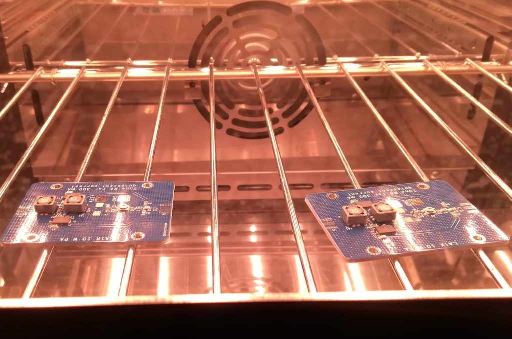
The first concern that presents itself is the solder-ability. AFM907N is slightly harder to deal with than the average amateur is normally used to. This is due to the exposed ground pad underneath the package, which means that the device must be soldered using hot air, or a solder oven. Our prototypes were made using the solder paste stencil and solder oven approach. We did end up having to touch up some of the joints with a soldering iron – a normal side-effect to doing pick and placement in caffeine withdrawal.
Once soldered, we were able to bring up the boards and make measurements.
We quickly learned that temperature runaway can be a very real concern with this amplifier. Having burnt one set of transistors to a unrestorable state, we came to realize that our lack of temperature compensation wasn’t all that clever.
Luckily we managed to calm things down using a 4.7 Ohm resistor in series with ground, allowing us to get some actual characteristics from the device. Note to future self (or other adopters) – add a proper temperature limited bias controller.
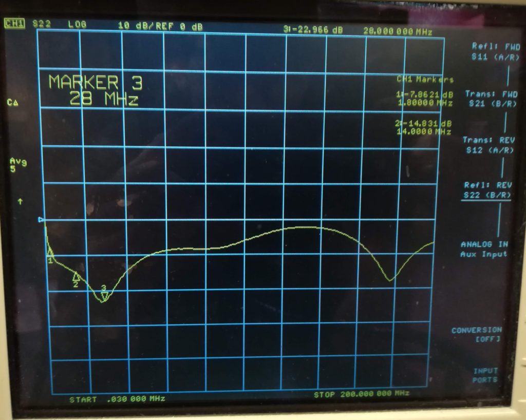
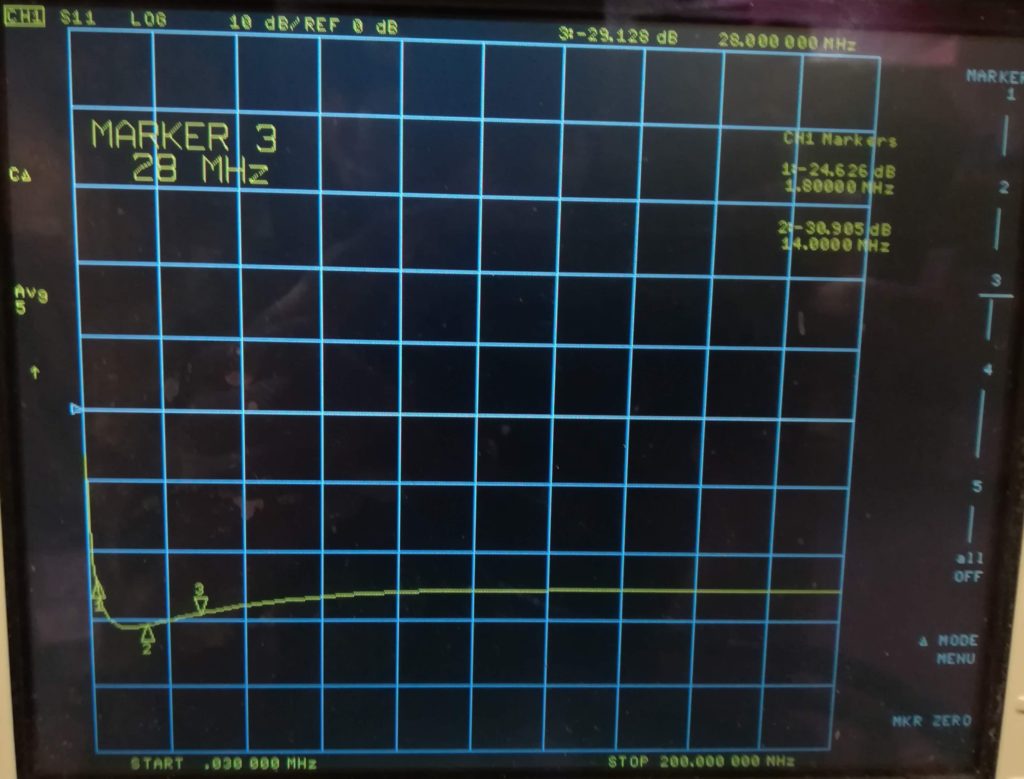
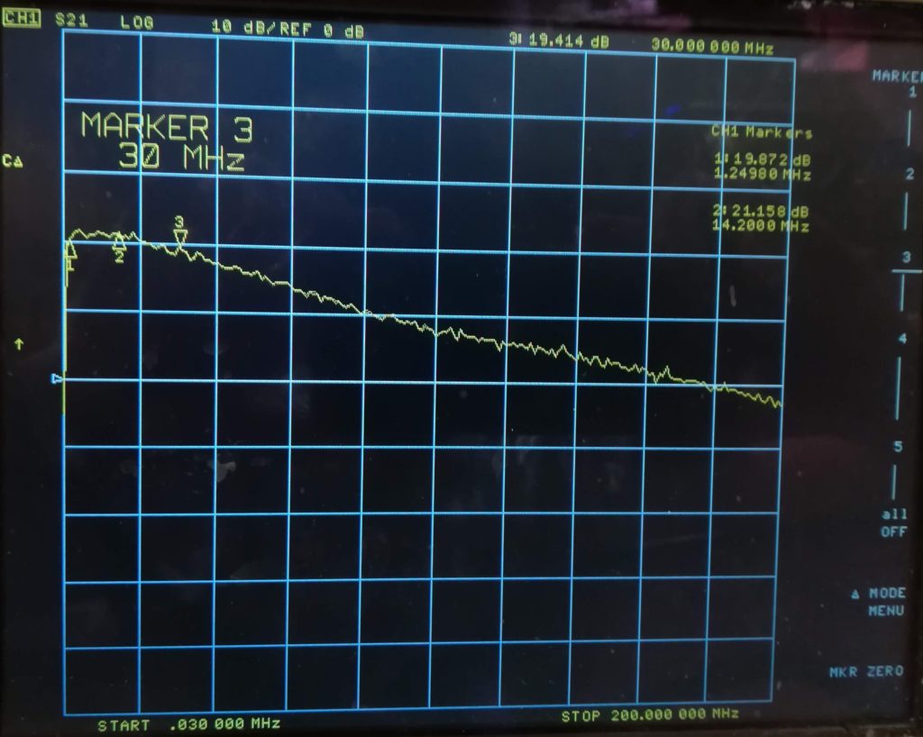
We got some actual results once that embarrassing ordeal was over. To our great satisfaction we got very nice correlation between simulated gain, and input/output match. Some implementation loss on the gain was found, on the order of 0.5-1 dB, although this is within the measurement accuracy.
The measurements were taken using two supplies: one for the drain voltage, and one to set the bias point. Gain and match were pretty stable across biases, given that the bias was sufficiently large (about 300 mA or above quiescent current).
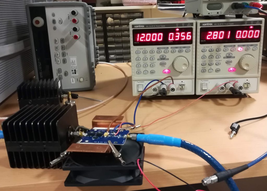
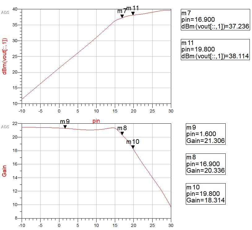
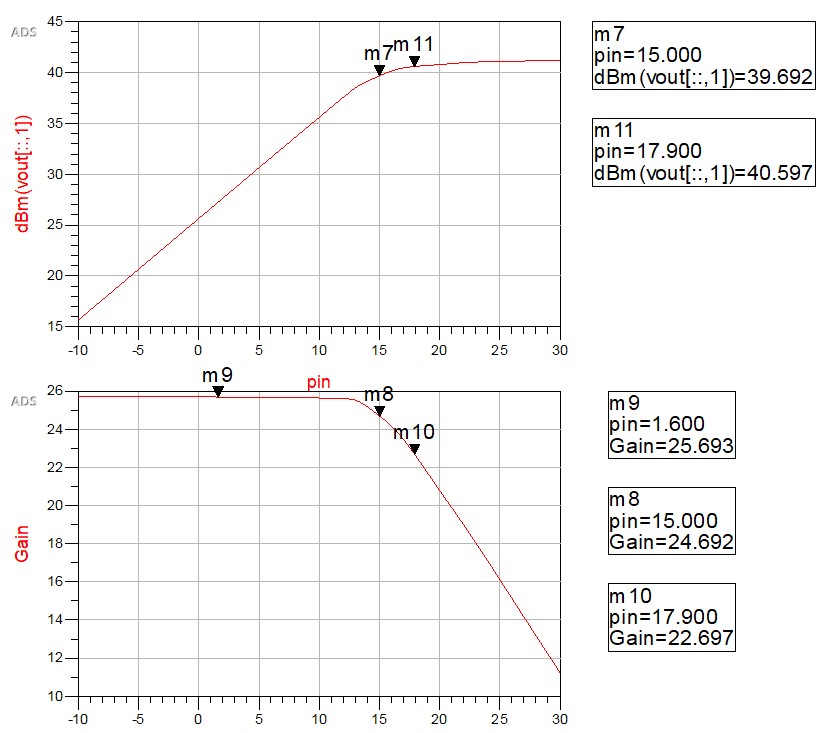
It was difficult to extract power from the device at the working points indicated by the simulations (seen below). Where the simulations favored higher voltage for higher output power, we found that the protoboard was much more happy given large current swing, with quiescent currents in the 1 A range. The simulation trend that favored higher voltage swing for more power also seemed less prevalent in the prototype. However, we did not take the time to fully assess this in combination with high quiescent currents.
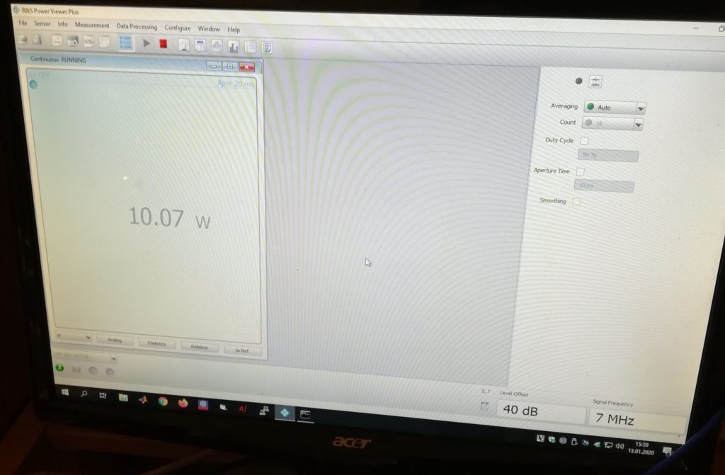
After some trimming, we achieved 10 W (1 dB compression) at 7 MHz. On the other HF bands, we got up to the 7-8 W range. For 50 MHz the power was down to 5 W. Nevertheless, we believe that with some extra coaxing, and carefully selected working points, we will be able to get very close to the desired 10 W point on all HF bands. We should also be able to get a bit better performance at 50 MHz.
We did not fully pursue 10 W output power across the board. This is because we ran into some issues with driving the amplifier hard enough, since our signal generator is limited to 20 dBm. A new implementation would probably benefit from revisiting the input match to increase overall amplifier gain. The current wye splitter input match is very simple, and performs well – but it is also very lossy.
Using a common mode choke as the match for the output stage was the part of the design that we were most apprehensive about. This seems to have worked out quite well, and the MSD7342-332 is more than up to the task. Thermals on the choke were low throughout our testing, indicating that losses in the choke were low.
Finally, the efficiency seems quite nice. At 10 W output power, the current draw is ~1.0 A from 12.5 V. If we include losses in the 4.7 Ohm ground resistor, this means that we are close to or above 50% efficiency.
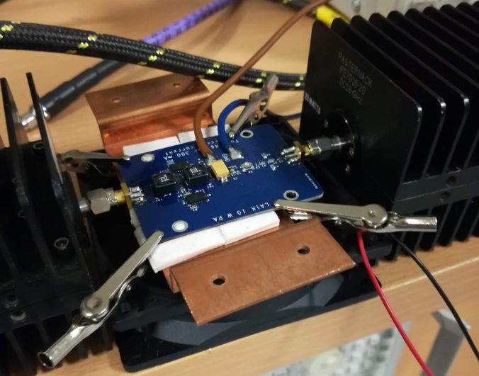
We were forced to use some additional heatsinking in order to keep the devices happy and cool, this can be seen in some of the pictures above. Mostly, this is due to the dramatic increase in heat dissipation when the devices are not driven. During amplification, each transistor only generates 1-2 W of heat, but when not driven this increases to 5-6 W. This is a side effect of running the transistors at such high quiescent currents.
Our opinion is that the AFM907N can make a very serviceable 10 W stage. Some things that should be explored further in a proper implementation are:
- Is the LDMOS is susceptible to long term electron migration effects when run at high voltages? To provoke such effects, a torture test can be conducted, e.g. 20 V 1 A operation for 7-8 hr cycles over the course of a week.
- A proper bias controller should be implemented. On a board with logical controls available the device would likely also benefit from having a 2-4 V trim range on the drain and 1-2 V on the gate.
- A less lossy input stage for more gain.
- Spurious content must be assessed to figure out how much filtering and backoff is needed to be compliant.
Overall we are very happy with the device and topology, and will put this neat trick in our toolkit. Perhaps it will show up as a driver or final stage in a future design. 🙂

You say, “we”, who else did this great work?
Mainly LA3WUA is involved in this particular project. We usually write “we” due to writing style considerations, regardless of the number of people involved.
Actually hams say, “we” because they lack self confidence to say, “I.”
Wasn’t this supposed to be a push-pull amplifier instead of a single ended design?
Originally that was the plan, however we ended up making a simpler mock up to be able to test it in the lab quickly. Might end up revisiting the push-pull idea if the amplifier makes it into a design.
Thank you for the clarification.